Google Targets Nvidia Software Lock-In With TPU 8tx and 8i Max
Google unveiled its TPU 8tx and TPU 8i Max systems alongside open-source TorchTPU and Oracle Cloud availability to reduce Nvidia CUDA switching costs.
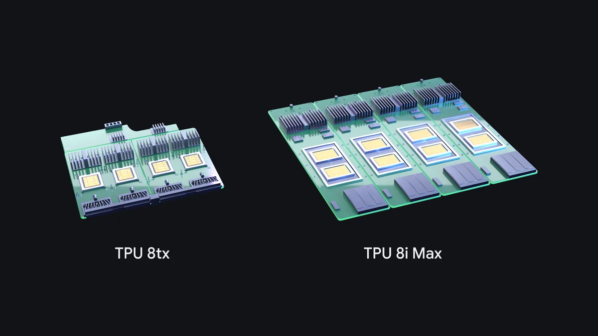
Competing against Nvidia in enterprise artificial intelligence has rarely been a matter of building a faster isolated processor. Google made that strategic reality explicit on November 9, 2026, in an official announcement on the Google Cloud Blog unveiling two new systems in its eighth-generation Tensor Processing Unit portfolio: TPU 8tx for hardware-level confidential computing and TPU 8i Max for massive-context agentic workloads.
Rather than waiting years for a new semiconductor lithography node, Google reorganized the eighth-generation silicon it first introduced at Google Cloud Next in April 2026 — TPU 8t for large-scale training and TPU 8i for real-time reasoning — into four specialized system configurations delivered within a single calendar year. Those hardware releases arrive alongside a broader platform offensive that pairs open-source native PyTorch execution with multicloud distribution through Oracle Cloud Infrastructure. Together, these moves show Google attempting to dismantle the software switching costs and single-cloud boundaries that have historically kept enterprise AI engineering locked inside the Nvidia GPU ecosystem.
Modular System Packaging Replaces Waiting for New Silicon Wafer Cycles
A central technical distinction in the November 9, 2026 release is that TPU 8tx and TPU 8i Max are new system configurations rather than two brand-new silicon architectures. As Amin Vahdat, Chief Technologist and Senior Vice President for AI and Infrastructure at Google, noted in the announcement, "there’s an important difference between a new chip and a new system."
Laying out billions of transistors on a fresh silicon wafer requires a multi-year manufacturing cycle, whereas re-architecting how existing dies are packaged with host processors, high-speed memory, optical networking, and hardware encryption lets engineers field specialized supercomputers in a matter of months. Building on the eighth-generation baseline — which delivers up to 12.6 PFLOPS of native FP4 compute per chip, up to 2.7 times higher training performance on TPU 8t, and an 80% inference price-performance gain on TPU 8i compared to the prior generation — the two new configurations target specific operational bottlenecks in enterprise production. TPU 8tx pairs the TPU 8t silicon with 5th Generation AMD EPYC CPU hosts and Google's low-latency Boardfly interconnect to keep sensitive data and model weights encrypted in memory during active processing, cutting latency by up to half compared to TPU 8t while letting regulated organizations run inference, private fine-tuning, model distillation, and reinforcement learning without moving confidential datasets across separate clusters.
| Eighth-Generation System | Base Silicon & Packaging | Documented Workload & Performance Parameters |
|---|---|---|
| TPU 8t | Eighth-generation training silicon (April 2026) | Foundation model pre-training; up to 2.7x training performance over prior generation and >97% goodput via ICI and OCS |
| TPU 8i | Eighth-generation inference silicon (April 2026) | Low-latency reasoning; 80% better inference price-performance over prior generation and up to 50% lower inter-chip delay |
| TPU 8tx | TPU 8t silicon with 5th Gen AMD EPYC CPU hosts | Hardware-level confidential inference, fine-tuning, and RL; Boardfly network cuts latency by up to 2x compared to TPU 8t |
| TPU 8i Max | Dual TPU 8i chips combined onto a single package | Massive context windows and multi-agent execution; 2x compute, 2x SRAM, and 2x HBM bandwidth within the same rack footprint |
While TPU 8tx addresses regulatory isolation, TPU 8i Max targets the memory bandwidth bottleneck that stalls autonomous agents when dozens of instances analyze an entire software repository or hours of video simultaneously. By combining two low-latency TPU 8i chips onto a single package, Google doubled compute capacity, on-chip SRAM, and High Bandwidth Memory (HBM) bandwidth in lockstep while fitting twice the silicon inside the existing rack footprint. Google reinforced that physical packaging on November 9, 2026 by releasing TPU Sync, an open-source C++ model-state library that links chip HBM, host DRAM, Google Cloud Managed Lustre storage, and data center networks into a unified memory hierarchy. In multi-turn agentic workloads and disaggregated prefill-decode serving, TPU Sync tiers large key-value (KV) caches off the accelerator in milliseconds, cutting KV transfer latency and Time to First Token (TTFT) by more than 90%, while a companion Agent Compute Engine suspends idle agent sessions waiting on external database lookups or human feedback.
Native PyTorch Execution and Open Serving Engines Target the CUDA Switching Cost
Hardware efficiency alone has never been sufficient to displace Nvidia in enterprise data centers because Nvidia's deepest competitive moat is CUDA and the surrounding software stack. Even when an alternative accelerator posts competitive throughput per watt, rewriting model code for custom compilers or debugging unfamiliar graph frameworks imposes an engineering switching cost that most organizations refuse to pay.
Google began attacking that software barrier directly on October 20, 2026, with the open-source release of TorchTPU at the PyTorch Conference 2026. Co-developed with the PyTorch engineering team at Meta and hosted on GitHub under google-pytorch/torch_tpu, TorchTPU treats the TPU as a native PyTorch device without wrapper types, supporting eager-mode debugging, torch.compile, and single-line deployment in Hugging Face Transformers v5 via device_map="tpu". Explaining why major AI operators pushed for this integration, Jana van Greunen, Director of PyTorch Engineering at Meta, stated on October 20, 2026, "We cannot be constrained by a single hardware architecture."
To extend that compatibility from model development into high-volume production serving and distributed training, Google partnered with Inferact to build a native vLLM-TorchTPU backend and collaborated with RadixArk on SGLang-TorchTPU, alongside integrations for Ray, VeRL, TorchTitan (validated at up to 52% Model Flops Utilization on Qwen 3 8B across 8,192 seventh-generation Ironwood TPUs), and an open-source TPU agent preview that plugs into coding environments such as native Jupyter notebooks in Google Antigravity to automate kernel tuning. Confirming that the open-source inference stack has already moved beyond laboratory testing, Zongwei Zhou, PyTorch-TPU Lead at Meta, noted on October 20, 2026 that "SGLang-TorchTPU is running in production at Meta" following a three-way engineering effort between Meta, Google, and the SGLang team.
Oracle Cloud Distribution and Q3 Revenue Growth Expand the Commercial Footprint
Lowering software friction solves only half of the adoption equation if enterprises still have to migrate their entire cloud footprint to Google Cloud just to rent TPU capacity. On October 27, 2026, at Oracle AI World in Las Vegas, Google and Oracle addressed that commercial bottleneck by announcing a partnership to deploy Google TPUs inside Oracle Cloud Infrastructure (OCI) starting in calendar year 2027, making OCI the first external hyperscaler to offer Google's custom accelerators. By connecting liquid-cooled TPU racks to Oracle databases and storage through Oracle Acceleron networking — which uses SmartNIC hardware tenant isolation and Zero Trust Packet Routing — the deal lets enterprises run fine-tuning and agentic inference directly beside their existing systems of record without cross-cloud data transfer fees.
Framing the commercial rationale for multi-architecture cloud environments, Mahesh Thiagarajan, President of Oracle Cloud Infrastructure, said on October 27, 2026, "Different AI workloads have different compute needs." For Google, turning OCI into a distribution channel transforms TPUs from an exclusive Google Cloud differentiator into portable infrastructure that can compete for workloads already anchored in third-party enterprise clouds.
Financial disclosures indicate that Google's custom silicon business is already generating substantial commercial volume prior to the 2027 Oracle rollout. According to the Alphabet Q3 2026 financial release filed with the SEC on October 28, 2026, Google Cloud revenue for the quarter ended September 30, 2026 rose 103% year over year to $30.709 billion, up from $15.157 billion in the third quarter of 2025, while segment operating income climbed from $3.594 billion to $11.121 billion. In the filing, Alphabet stated that "TPU systems sales were also a meaningful contributor to revenue growth" and specified in its segment notes that Google Cloud generates product revenues primarily from the sale of TPU systems — a business that Amin Vahdat reported on November 9, 2026 now serves nearly 100 customers across frontier AI labs, trading firms, retailers, and universities, including direct deployments inside customer-owned data centers.
Independent Benchmark Audits and Unanswered Pricing Questions Ahead of 2027
Alphabet's SEC filings and technical blogs still leave four material questions unanswered for engineering teams evaluating whether TPU 8tx and TPU 8i Max can capture share from Nvidia. First, Alphabet does not break out standalone TPU product revenue or unit margins within Google Cloud's $30.709 billion quarterly total, and Google has not published hourly instance rates or comparable cost-per-million-token pricing for the new TPU 8tx and TPU 8i Max systems.
Second, while Google cites strong production results on the SemiAnalysis InferenceX and AgentX benchmarks — which evaluate multi-turn agentic coding and long-context prefix caching much like structured web-grounded agent lookups on OpenRouter and generalization testing on the MaxxBench benchmark — the specific milestones published by Google's engineering team on October 20, 2026 (including a cost of 2.01 cents per million tokens on Qwen 3.5 and more than 700 tokens per second for a single user on the 2.8-trillion-parameter Kimi K3 model) were recorded on seventh-generation Ironwood TPU v7x hardware. The public InferenceX hardware matrix currently lists TPU7x alongside Nvidia's H100, H200, B200, B300, GB200 NVL72, GB300 NVL72, and Vera Rubin NVL72 systems, meaning independent GitHub Actions benchmark runs for the eighth-generation TPU 8tx and TPU 8i Max configurations have yet to be posted. As Google rolls out GKE dynamic slicing and Cloud Pathways into general availability and prepares to bring TPU capacity online inside Oracle Cloud Infrastructure in 2027, external adoption will depend on verified eighth-generation price-performance audits, HBM supply scale, and sustained PyTorch stability under real enterprise production loads.

Written by Adriano Nascentes
Founder & Lead AI Systems Analyst · Verified Staff
Founder and editor-in-chief of Unknown Observer. Technology researcher and software engineer investigating foundation models, autonomous agent runtimes, cognitive architectures, and frontier AI safety.
Was this article helpful?
Your feedback helps our editorial team refine reporting depth and accuracy.